Getting Started with PCB Design: A Comprehensive Guide for Beginners
2026-03-19 16:43:22
Printed Circuit Boards (PCBs) are the backbone of modern electronics. From simple LED drivers to complex computer processors, every electronic device relies on PCBs to connect components and create functional circuits. This comprehensive guide will walk you through everything you need to know to start designing your own PCBs, whether you are a hobbyist or an aspiring hardware engineer.
What is a PCB?
A Printed Circuit Board is a laminated structure made of insulating material (typically FR-4) with conductive copper traces etched onto its surface. These traces connect electronic components mounted on the board, eliminating the need for messy point-to-point wiring. PCBs provide mechanical support and electrical connections, making them essential for reliable electronic products.
Understanding PCB Layers
PCBs come in different layer configurations, each suited for different applications and complexity levels.
Single-Layer PCBs
Also known as single-sided PCBs, these boards have copper traces on only one side of the substrate. They are the simplest and most cost-effective option, ideal for simple circuits like power supplies and basic consumer electronics. The main limitation is that component placement and routing are restricted to one side, which can result in longer trace routes.
Double-Layer PCBs
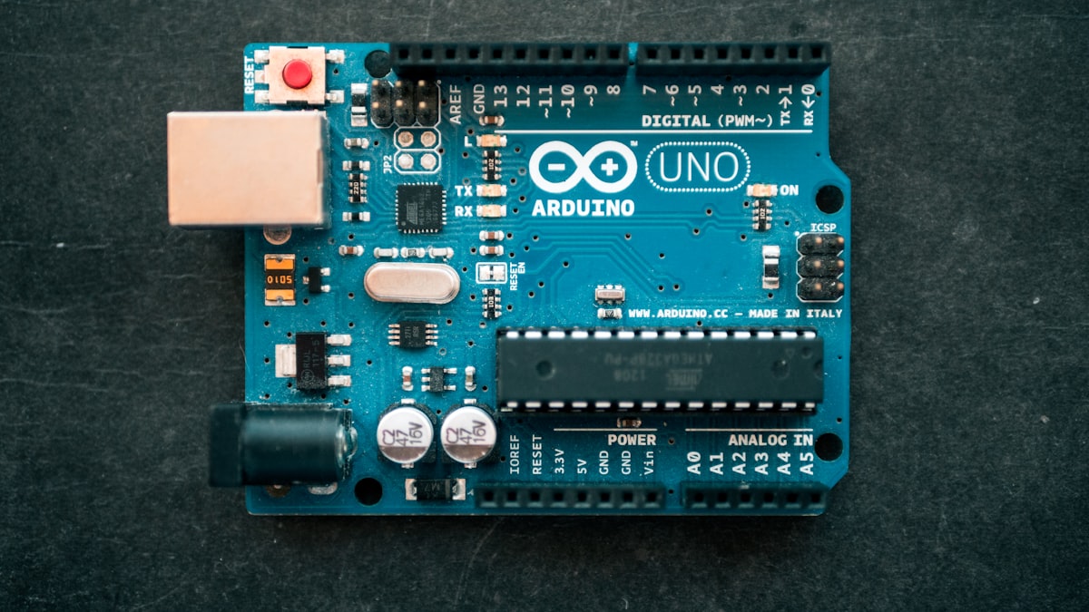
Double-sided PCBs have copper traces on both sides of the substrate, allowing for more complex designs. Vias (plated through-holes) connect traces between layers, enabling more efficient component placement and shorter signal paths. These boards are suitable for most hobbyist projects and many commercial applications.
Multi-Layer PCBs
Multi-layer PCBs consist of multiple insulating layers sandwiched between conductive layers. Common configurations include 4-layer, 6-layer, and 8-layer boards. These are used in sophisticated applications like computers, smartphones, and communications equipment where signal integrity and compact size are critical.
Key PCB Design Steps
Step 1: Schematic Design
Every PCB starts with a schematic—a graphical representation of the circuit showing all components and their electrical connections. A well-drawn schematic is crucial for successful PCB design.
Key considerations:
- Component symbols: Use standard library symbols for clarity
- Net names: Label critical nets (power, ground, signals)
- Reference designators: Assign unique identifiers (R1, C2, U3) to each component
- Power and ground: Clearly indicate all power rails and ground connections
Step 2: Component Selection and Placement
After completing the schematic, you need to select specific components and place them on the board. Component placement significantly impacts circuit performance, manufacturability, and cost.
Placement Guidelines:
- Place decoupling capacitors close to IC power pins
- Group related components together (e.g., USB circuitry)
- Keep high-speed signals short and direct
- Consider thermal management for power components
- Leave space for connectors and mounting holes
Step 3: Routing
Routing involves creating copper traces to connect components according to the schematic. This step requires careful attention to signal integrity, current capacity, and manufacturing constraints.
PCB Design Rules and Constraints
Understanding design rules is essential for creating manufacturable and reliable PCBs.
| Parameter | Standard PCB | Fine-Pitch PCB | Notes |
|---|---|---|---|
| Minimum Trace Width | 0.15mm (6mil) | 0.1mm (4mil) | Depends on current capacity |
| Minimum Spacing | 0.15mm (6mil) | 0.1mm (4mil) | Important for voltage isolation |
| Via Diameter | 0.3mm (12mil) | 0.2mm (8mil) | Drill size + plating thickness |
| Via Annular Ring | 0.15mm (6mil) | 0.1mm (4mil) | Minimum copper ring around via |
| Minimum Hole Size | 0.3mm | 0.2mm | Limited by drill tooling |
PCB Materials: FR-4 and Beyond
The substrate material determines the PCBs electrical and mechanical properties. FR-4 (Flame Retardant 4) is the most common material, but other options exist for specialized applications.
| Material | Tg (C) | Dielectric Constant | Applications |
|---|---|---|---|
| FR-4 Standard | 130-140 | 4.2-4.8 | General purpose, cost-effective |
| FR-4 High Tg | 170-180 | 4.2-4.8 | Lead-free assembly, thermal stress |
| Rogers RO4003 | 280+ | 3.38 | RF, microwave, high-frequency |
| Polyimide | 250-260 | 3.2-3.6 | Flexible circuits, high-temp apps |
Popular PCB Design Software
Choosing the right design tool is crucial. Here is a comparison of popular options for beginners and professionals.
| Software | Cost | Learning Curve | Best For |
|---|---|---|---|
| EasyEDA | Free (starter) | Easy | Hobbyists, quick prototypes |
| KiCad | Free (open-source) | Medium | Open-source projects, students |
| Altium Designer | 2,500+/year | Steep | Professional, complex designs |
| Fusion 360 | 545/year | Medium | Hobbyists to pros |
From Design to Manufacturing
Once your design is complete, you need to generate manufacturing files (Gerber files) and send them to a PCB fab house. Here is the typical workflow:
Generating Gerber Files
Gerber files are the industry-standard format for PCB manufacturing. Your design software can export:
- Top Copper (GTL) - Top layer traces
- Bottom Copper (GBL) - Bottom layer traces
- Silkscreen (GTO/GBO) - Component outlines and reference designators
- Solder Mask (GTS/GBS) - Green (or other color) solder mask opening
- Drill File (XL) - Hole locations and sizes
- NC Drill - Numerical control drill instructions
Example Gerber File Header:
%FSLAX46Y46*%
%MOMM*%
%ADD11R,0.8X1.2X0.0*%
%ADD12C,0.5*%
G01*
X0Y0D02*
X1000Y500D01*
...
Design for Manufacturing (DFM) Checklist
Before sending your files to manufacture, verify these common issues:
- All traces meet minimum width and spacing rules
- Via annular rings are sufficient (minimum 0.15mm)
- Copper-to-edge clearance is adequate (minimum 0.2mm)
- Silkscreen text does not overlap pads
- Drill holes have sufficient margin from traces
- All keep-out areas are properly defined
Best Practices for Beginners
- Start Simple: Begin with single-layer boards before attempting multi-layer designs
- Follow Design Rules: Use your software design rule checker (DRC) consistently
- Keep Grounds Solid: Use polygon pours for ground planes to reduce noise
- Label Your Board: Add silkscreen text for version, date, and project name
- Document Everything: Keep notes on design decisions and component choices
- Order Prototypes: Test your design with low quantities before full production
- Learn from Mistakes: Every failed prototype is a learning opportunity
Common Pitfalls to Avoid
- Insufficient clearance: Short circuits between traces are common errors
- Forgot decoupling capacitors: Place 100nF caps near every IC power pin
- Ignoring thermal relief: Large pads need proper thermal relief for soldering
- Wrong component footprint: Always verify footprint dimensions before ordering
- No ground plane: Digital circuits need solid ground planes for noise immunity
Conclusion
PCB design is both an art and a science. While the fundamentals are straightforward, creating reliable, manufacturable designs takes practice and attention to detail. Start with simple projects, gradually increasing complexity as you gain experience. Remember to always verify your designs with design rule checks and manufacturer capabilities.
The skills you develop through PCB design will open doors to countless DIY electronics projects, prototype development, and potentially a career in hardware engineering. With the availability of affordable PCB fabrication services, there has never been a better time to start learning PCB design.
Ready to start your PCB project?
Need help with component selection or manufacturing? Our team has extensive experience in PCB design and can help bring your ideas to life.
Get a Quote
Last updated: March 2026